
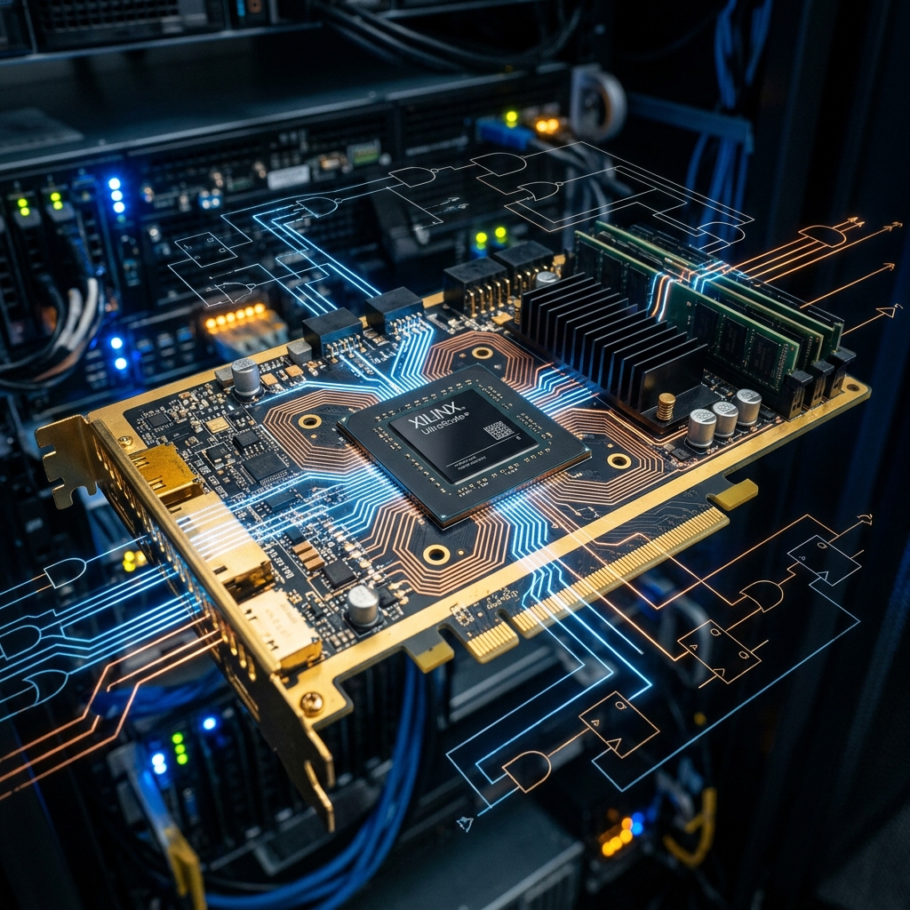
1. Introduction: The Physical Reality of Latency
In high-frequency trading (HFT), execution speed is constrained by the physics of computation. When a market event occurs—such as a large trade filling the best bid on CME—the update travels as an electrical or optical signal to the colocation data center. If your trading pipeline relies on traditional software architectures, this packet must pass through the network card, trigger an interrupt, traverse the operating system kernel, and be processed by a CPU execution thread.
Even with optimizations like **Kernel Bypass (DPDK/Solarflare OpenOnload)** and thread pinning, a CPU-based tick-to-trade cycle takes several microseconds. In that time window, FPGA-driven predatory algorithms have already decoded the packet, evaluated risk constraints in hardware, and crossed the queue. To preserve alpha in highly volatile environments, quantitative firms must replace general-purpose CPUs with custom-designed hardware bitstreams executing directly inside **Field-Programmable Gate Arrays (FPGAs)**.
2. CPU vs. FPGA Processing Pipelines
A standard CPU executes instructions sequentially, relying on memory caches (L1/L2/L3) and thread schedulers. In contrast, an FPGA consists of a reconfigurable fabric of physical logic blocks (Look-Up Tables, Flip-Flops, Block RAM) and DSP slices. An FPGA does not run software; it behaves as a dedicated hardware circuit optimized for a single task.
The table below illustrates the latency differences at each stage of a typical tick-to-trade pipeline comparing optimized C++ code with hardware FPGA gate structures:
| Pipeline Stage | C++ Software (Kernel Bypass) | FPGA Hardware Bitstream | Speed Advantage |
|---|---|---|---|
| Packet Ingestion (SBE/FIX) | 450 - 900 ns | 40 - 80 ns | ~10x faster |
| Book Building (Depth Update) | 800 - 1500 ns | 120 - 180 ns | ~8x faster |
| Alpha Model Evaluation | 1200 - 4500 ns | 150 - 350 ns | ~12x faster |
| Pre-Trade Risk Checking | 350 - 800 ns | 30 - 50 ns | ~15x faster |
| Order Serialization (FIX/OUCH) | 600 - 1200 ns | 45 - 90 ns | ~13x faster |
3. The Architecture of an FPGA Feed Handler
To implement hardware acceleration, the entire logic pathway must be translated into hardware elements. The pipeline is designed as a series of stream-processing stages:
A. MAC/PCS Layer
Optical signals from exchange fibers enter the FPGA's SFP+/QSFP transceivers. The Physical Coding Sublayer (PCS) and Medium Access Control (MAC) block parse raw Ethernet frames directly at electrical clock cycles, typically outputting 64-bit or 128-bit words over an AXI-Stream interface on every clock tick (e.g., at 322.26 MHz for a 10GbE interface, yielding 3.1 ns per tick).
B. Protocol Parser (SBE / FIX / FAST)
Rather than copying buffers, a state-machine parses the stream byte-by-byte as it flows through the FPGA. Simple Binary Encoding (SBE) fields are extracted using bitwise masks. If the packet describes an update at a price level we track, the fields are passed immediately to the internal book builder.
C. Parallel Book Building
FPGAs maintain order book arrays inside Block RAM (BRAM). Depth updates are processed in parallel. If an incoming message updates Level 1 Ask, the FPGA simultaneously: (1) updates the local BRAM memory, (2) recalculates internal volatility values, and (3) signals the order evaluator if an alpha condition is triggered.
4. Pre-Trade Risk Checks: Logic Gate Constraints
Exchanges require that every order pass rigorous pre-trade risk checks (e.g., maximum order size, price deviation limits, credit limits). In software, evaluating these safety checks requires reading variables, verifying constraints, and executing conditional branches, taking up valuable time.
In an FPGA bitstream, risk parameters are hardwired as logic circuits. For example, verifying that a proposed trade size $Q$ does not exceed maximum limit $L$ is evaluated by feeding $Q$ and $L$ directly into a physical array of digital comparators. The comparison takes exactly one clock cycle (under 3 nanoseconds). If any safety condition is violated, the bitstream immediately drops the trade packet, preventing erroneous execution without affecting the pipeline's latency when trades are valid.
5. High-Level Synthesis (HLS) C++ Risk Evaluator
While HFT engineers historically coded bitstreams in Verilog or VHDL, modern architectures utilize High-Level Synthesis (HLS) to compile C++ code structures directly into silicon RTL logic gates. The following code block illustrates an optimized HLS C++ risk checker utilizing pragmas to force pipelining and single-cycle executions:
#include <ap_int.h>

struct Order {
    ap_uint<32> price;
    ap_uint<32> quantity;
    ap_uint<8>  side; // 0 = Buy, 1 = Sell
};

struct RiskConfig {
    ap_uint<32> maxQuantity;
    ap_uint<32> priceThreshold;
};

// High-Level Synthesis HFT Risk Evaluator
// Compiles directly to FPGA RTL logic gates with a latency of 1 clock cycle
bool evaluateRiskRules(const Order& order, const RiskConfig& config, ap_uint<32> currentBestBid) {
    #pragma HLS PIPELINE II=1
    #pragma HLS INTERFACE ap_none port=order
    #pragma HLS INTERFACE ap_none port=config
    #pragma HLS INTERFACE ap_none port=currentBestBid

    // Rule 1: Validate trade size limit
    bool sizeOk = (order.quantity <= config.maxQuantity);

    // Rule 2: Prevent buying at excessively high prices relative to current bid
    bool priceOk = true;
    if (order.side == 0) {
        ap_uint<32> maxAllowedPrice = currentBestBid + config.priceThreshold;
        priceOk = (order.price <= maxAllowedPrice);
    }

    // Combine rules using parallel physical gate paths
    return (sizeOk && priceOk);
}
6. Dynamic Re-Configuration and Hybrid Execution
Deploying pure FPGA pipelines introduces a trade-off: hardware speeds are unmatched, but silicon logic is extremely difficult to update. Re-compiling a complex FPGA bitstream takes several hours, whereas trading models must adapt to volatile market conditions continuously.
To balance speed and agility, TwoWayMind's execution engine utilizes a Hybrid FPGA-CPU Co-Processor Architecture. Our feed handlers and pre-trade risk evaluation logic are locked inside FPGA silicon gates to guarantee sub-microsecond tick-to-trade latency. However, the pricing models and alpha weights are computed by CPUs in C++ and written dynamically to the FPGA's registers over a PCIe DMA bypass. This design allows our quantitative algorithms to update strategy logic on the fly while maintaining deterministic, nanosecond-level execution speeds when opportunities appear.